This post is the final in my series on creating an Advanced Encryption Standard encryption implementation in configurable digital logic for the Zynq7000 FPGA. In this post. In this post, I'll describe the finalized firmware and software implementation. This exercise provided (in my opinion) an excellent means of learning to create configurable digital logic firmware and integrate it into a practical system design on hardware. The complete firmware and software implementation can be found in the repository linked at the top of this page.
(On a side note, my CDL journey really started with learning how to blink some LEDs in this post and by implementing the DES encryption algorithm in verilog in this series. )
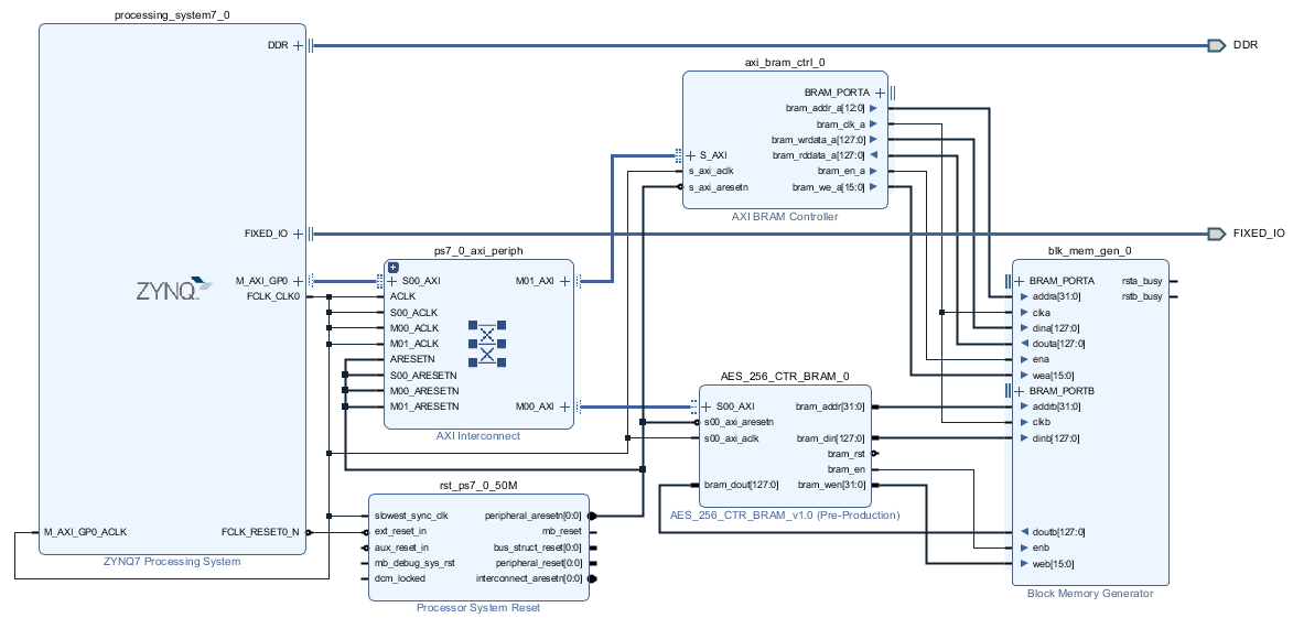
The finalized AES CTR module is designed to provide a hardware accelerated encryption service to an application running on a conventional processor. I implemented this project on the Zynq7000 FPGA. The AES CTR module resides in the FPGA fabric, alongside a block memory region mapped to an address space accessible to the processing system. An AXI-4 memory mapped interface is provided to the software for command-and-control of the AES module. The processor utilizes the encryption service by writing data to the block RAM, configuring the AES module with the key, initialization vector, and base address, and subsequently enabling the module. The module reports when the operation is complete through a status register. The diagram below is a simplified version of the system block design.
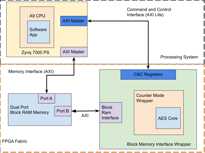
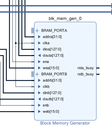
The memory interface between the processing system and the AES CTR module was implemented via a block RAM residing in the FPGA fabric. The block RAM was implemented with the Xilinx Block Memory Generator IP. The block was configured as a dual-port RAM with a 128-bit read and write width to match the size of an AES data block. Port A was connected to the Zynq7000 PS AXI master 0 via AXI interconnect and Xilinx AXI Block RAM controller IP block. Port B was connected to the AES CTR module BRAM interface.
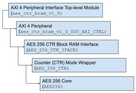
The AES CTR module is the heart of the system design. It is implemented as an AXI-4 Lite module and packaged as IP in its own project. It consists of the AES ECB core, the CTR mode wrapper, and the block RAM interface wrapper. The module provides an AXI-4 Lite slave interface for command-and-control registers and a block RAM interface for reading and writing to and from memory that is mapped and accessible to the processing system. The packaged IP was added to the system block design. The slave interface was connected, via AXI interconnect, to the Zynq7000 processing system's AXI general purpose master 0. The block RAM interface was connected to one port of a block RAM controller provided by the Xilinx Block Memory Generator IP.
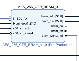
The AXI wrapper around the AES CTR module was created using Xilinx Vivado's "Create and Package IP" feature. First, the necessary ports were added to the automatically generated AXI-4 peripheral interface module.
output wire [31:0] bram_addr,   //BRAM Address
output wire [127:0] bram_din,   //BRAM data in
input  wire [127:0] bram_dout,  //BRAM data out
output wire bram_en,            //BRAM enable
output wire bram_rst,           //BRAM reset
output wire [31:0] bram_wen,    //BRAM write enable
bram_addr - This port is the address output to the block RAMbram_din - This port outputs write data to the block RAM data-in portbram_dout - This port receives data from the block RAM data-out portbram_en - This output enables or disables the block RAMbram_rst - This port is used for resetting the block RAMbram_wen - This port is the write-enable for the block RAMThese ports were wired into corresponding ports added to the auto-generated AXI peripheral module.
    .bram_addr(bram_addr),
    .bram_din(bram_din),
    .bram_dout(bram_dout),
    .bram_en(bram_en),
    .bram_rst(bram_rst),
    .bram_wen(bram_wen)
);
Inside the AXI peripheral module, the above ports were added to the module declaration.
    // Users to add ports here
    output wire [31:0] bram_addr,   //BRAM Address
    output wire [127:0] bram_din,   //BRAM data in
    input  wire [127:0] bram_dout,  //BRAM data out
    output wire bram_en,            //BRAM enable
    output wire bram_rst,           //BRAM reset
    output wire [31:0] bram_wen,    //BRAM write enable
Registers were added for the AES CTR Interface module, and the module was instantiated.
	//AES Interface Module
	reg enable;
	reg resetn;
	reg [255:0] key;
	reg [127:0] iv;
	reg [31:0] base_addr;
	reg [31:0] num_blocks;
	wire done;

	AES_256_CTR_IFACE aes_iface
		(
			.clock(S_AXI_ACLK),
			.enable(enable),
			.resetn(resetn),
			.key(key),
			.iv(iv),
			.base_addr(base_addr),
			.num_blocks(num_blocks),
			.bram_addr(bram_addr),
			.bram_din(bram_din),
			.bram_dout(bram_dout),
			.bram_en(bram_en),
			.bram_rst(bram_rst),
			.bram_wen(bram_wen),
			.done(done)
		);
The AES CTR command-and-control registers were mapped (summarized below) to corresponding AXI slave registers in the AXI-read logic of the module.
	begin
	      // Commmand and control register reads
	      case ( axi_araddr[ADDR_LSB+OPT_MEM_ADDR_BITS:ADDR_LSB] )
	        4'h0   : reg_data_out <= 32'h20211130; //Version, sanity check register
	        4'h1   : reg_data_out <= {29'b0, done, resetn, enable}; //IOs
	        4'h2   : reg_data_out <= key[255:224]; //key w0 //MSW
	        4'h3   : reg_data_out <= key[223:192]; //key w1 12
	        4'h4   : reg_data_out <= key[191:160]; //key w2 16
	        4'h5   : reg_data_out <= key[159:128]; //key w3 20
	        4'h6   : reg_data_out <= key[127:96];  //key w4	24
	        4'h7   : reg_data_out <= key[95:64];   //key w5	28
	        4'h8   : reg_data_out <= key[63:32];   //key w6 32
	        4'h9   : reg_data_out <= key[31:0];    //key w7 //LSW
	        4'hA   : reg_data_out <= iv[127:96];   //IV w0 //MSW
	        4'hB   : reg_data_out <= iv[95:64];    //IV w1 44
	        4'hC   : reg_data_out <= iv[63:32];    //IV w2 48
	        4'hD   : reg_data_out <= iv[31:0];     //IV w3 //LSW
	        4'hE   : reg_data_out <= num_blocks;   //number of blocks
	        4'hF   : reg_data_out <= base_addr;    //block ram base address
	        default : reg_data_out <= 0;
	      endcase
	end
An always block was added to map the AXI slave register values to the input registers of the AES CTR module.
//command-and-control register writes
always @(posedge S_AXI_ACLK)
begin
    enable       <= slv_reg1[0];      //Enable signal
    resetn       <= slv_reg1[1];      //Reset (low)
    key[255:224] <= slv_reg2;         //key w0 //MSW
    key[223:192] <= slv_reg3;         //key w1
    key[191:160] <= slv_reg4;         //key w2
    key[159:128] <= slv_reg5;         //key w3
    key[127:96]  <= slv_reg6;         //key w4
    key[95:64]   <= slv_reg7;         //key w5
    key[63:32]   <= slv_reg8;         //key w6
    key[31:0]    <= slv_reg9;         //key w7 //LSW
    iv[127:96]   <= slv_reg10;        //IV w0 //MSW
    iv[95:64]    <= slv_reg11;        //IV w1
    iv[63:32]    <= slv_reg12;        //IV w2
    iv[31:0]     <= slv_reg13;        //IV w3 //LSW
    num_blocks   <= slv_reg14;        //number of blocks
    base_addr    <= slv_reg15;        //block ram base address
end
The following table provides a summary of the command-and-control registers.
| Register | Offset | Read/Write | Description | Bit Definitions |
|---|---|---|---|---|
| Version Register | 0x0 | RO | Returns a 32-bit hex version tag in the date format YYYYMMDD | - |
| Status and Control Register | 0x4 | W | Write reset and enable signals | Reserved (29),DONE, RESET LOW, ENABLE |
| Control Register | 0x4 | R | Read DONE signal | |
| KEY_0 | 0x8 | WO | 32-bit Key Word 0 (big-endian most significant four bytes) | - |
| KEY_1 | 0xC | WO | 32-bit Key Word 1 | - |
| KEY_2 | 0x10 | WO | 32-bit Key Word 2 | - |
| KEY_3 | 0x14 | WO | 32-bit Key Word 3 | - |
| KEY_4 | 0x18 | WO | 32-bit Key Word 4 | - |
| KEY_5 | 0x1C | WO | 32-bit Key Word 5 | - |
| KEY_6 | 0x20 | WO | 32-bit Key Word 6 | - |
| KEY_7 | 0x24 | WO | 32-bit Key Word 7 (big-endian least significant four bytes) | - |
| IV_0 | 0x28 | WO | 32-bit IV Word 0 (big-endian most significant four bytes) | - |
| IV_1 | 0x2C | WO | 32-bit IV Word 1 | - |
| IV_2 | 0x30 | WO | 32-bit IV Word 2 | - |
| IV_3 | 0x34 | WO | 32-bit IV Word 3 (big-endian least significant four bytes) | - |
| NUM_BLOCKS | 0x38 | WO | Number of AES blocks to process | - |
| BASE_ADDR | 0x3C | WO | - |
The image below shows the final block design used for testing and verification of the AES CTR module.
The ultimate goal of this module is to provide a software application running in the Zynq7000 processing system with a hardware accelerated encryption service. A proof-of-concept software application, including a software API for the AES module, was created.
The generated hardware platform memory map places the block RAM region at address 0x40000000. The AES CTR module command-and-control interface is mapped to 0x43c00000. Although most of it is boilerplate, the memory map is included in the table below for completeness.
| Device | Base Address | High Address | Slave Interface | Addr Range Type |
|---|---|---|---|---|
| ps7_intc_dist_0 | 0xf8f01000 | 0xf8f01fff | - | register |
| ps7_scutimer_0 | 0xf8f00600 | 0xf8f0061f | - | register |
| ps7_slcr_0 | 0xf8000000 | 0xf8000fff | - | register |
| ps7_scuwdt_0 | 0xf8f00620 | 0xf8f006ff | - | register |
| AES_256_CTR_BRAM_0 | 0x43c00000 | 0x43c0ffff | S00_AXI | register |
| ps7_l2cachec_0 | 0xf8f02000 | 0xf8f02fff | - | register |
| ps7_scuc_0 | 0xf8f00000 | 0xf8f000fc | - | register |
| ps7_pmu_0 | 0xf8893000 | 0xf8893fff | - | register |
| ps7_afi_1 | 0xf8009000 | 0xf8009fff | - | register |
| ps7_afi_0 | 0xf8008000 | 0xf8008fff | - | register |
| ps7_afi_3 | 0xf800b000 | 0xf800bfff | - | register |
| ps7_afi_2 | 0xf800a000 | 0xf800afff | - | register |
| ps7_globaltimer_0 | 0xf8f00200 | 0xf8f002ff | - | register |
| ps7_dma_s | 0xf8003000 | 0xf8003fff | - | register |
| ps7_iop_bus_config_0 | 0xe0200000 | 0xe0200fff | - | register |
| ps7_xadc_0 | 0xf8007100 | 0xf8007120 | - | register |
| ps7_ddr_0 | 0x00100000 | 0x1fffffff | - | memory |
| ps7_ddrc_0 | 0xf8006000 | 0xf8006fff | - | register |
| ps7_ocmc_0 | 0xf800c000 | 0xf800cfff | - | register |
| ps7_pl310_0 | 0xf8f02000 | 0xf8f02fff | - | register |
| ps7_uart_1 | 0xe0001000 | 0xe0001fff | - | register |
| ps7_coresight_comp_0 | 0xf8800000 | 0xf88fffff | - | register |
| axi_bram_ctrl_0 | 0x40000000 | 0x40001fff | S_AXI | memory |
| ps7_scugic_0 | 0xf8f00100 | 0xf8f001ff | - | register |
| ps7_dev_cfg_0 | 0xf8007000 | 0xf80070ff | - | register |
| ps7_dma_ns | 0xf8004000 | 0xf8004fff | - | register |
| ps7_gpv_0 | 0xf8900000 | 0xf89fffff | - | register |
| ps7_ram_1 | 0xffff0000 | 0xfffffdff | - | memory |
| ps7_ram_0 | 0x00000000 | 0x0002ffff | - | memory |
A simple software module was created to facilitate register reads and writes. The register addresses were defined as an enumeration, and read and write functions were declared in the header.
///This enum is the register memory mapping
typedef enum
{
    AES_CTRL_BASE      = 0x43c00000,
    VERSION_REG        = (AES_CTRL_BASE),
    STATUS_CTRL_REG    = (AES_CTRL_BASE + 4),
    KEY_0              = (AES_CTRL_BASE + 8),
    KEY_1              = (AES_CTRL_BASE + 12),
    KEY_2              = (AES_CTRL_BASE + 16),
    KEY_3              = (AES_CTRL_BASE + 20),
    KEY_4              = (AES_CTRL_BASE + 24),
    KEY_5              = (AES_CTRL_BASE + 28),
    KEY_6              = (AES_CTRL_BASE + 32),
    KEY_7              = (AES_CTRL_BASE + 36),
    IV_0               = (AES_CTRL_BASE + 40),
    IV_1               = (AES_CTRL_BASE + 44),
    IV_2               = (AES_CTRL_BASE + 48),
    IV_3               = (AES_CTRL_BASE + 52),
    NUM_BLOCKS         = (AES_CTRL_BASE + 56),
    BASE_ADDR          = (AES_CTRL_BASE + 60)
}REGISTER;

///This function is for reading registers
extern uint32_t reg_read(REGISTER reg);

///This function is for writing registers
extern void reg_write(REGISTER reg, uint32_t val);
The corresponding functions were defined in the source file of the module.
#include "registers.h"

uint32_t reg_read(REGISTER reg)
{
    return *(uint32_t*)reg;
}

void reg_write(REGISTER reg, uint32_t val)
{
    *(uint32_t*)reg = val;
}
A software module was created to provide a software API to the AES CTR module. Two definitions were added for the 32-bit word length of a 256-bit AES key and 128-bit Initialization Vector, and an encrypt and decrypt function were declared in the header.
#define AES_256_KEY_WORDS 8
#define AES_256_IV_WORDS  4

///This function performs encryption of the source buffer,
///writing the output into the destination buffer.
extern void aes256Ctr_encrypt(uint32_t * dest,
                              uint32_t * src,
                              uint32_t num_words,
                              uint32_t * key,
                              uint32_t * iv);

///This function performs decryption of the source buffer,
///writing the output into the destination buffer.
extern void aes256Ctr_decrypt(uint32_t * dest,
                              uint32_t * src,
                              uint32_t num_words,
                              uint32_t * key,
                              uint32_t * iv);
dest - A pointer to the memory where the output of the encrypt or decrypt operation will be storedsrc - A pointer to the data to be encrypted or decryptednum_words - The number of 32-bit words to be encrypted or decryptedkey - A pointer to the 256-bit AES keyIV - A pointer to the 128-bit AES Initialization VectorThe AES software module source file contains definitions for the base address of the block RAM memory region (corresponding to that in the memory map), the bit sequence to release the AES CTR module from reset, the bit sequence to enable the AES CTR module, and the position of the done bit in the status register.
#define AES_MEM_BASE  0x40000000 //!< Base address of the AES BRAM
#define RELEASE 0b10             //!< Release AES CTR from reset
#define ENABLE  0b11             //!< Enable AES CTR module
#define DISABLE 0                //!< Disabel AES CTR module
#define DONE_BIT 0b100           //!< Done bit position
The encrypt and decrypt functions were defined in the body of the AES software module. The first step releases the AES CTR module from reset.
    //Take AES module out of reset
    reg_write(STATUS_CTRL_REG, RELEASE);
Next, the key is populated into the key registers, followed by the IV.
    //Set up the key
    reg_write(KEY_0, key[0]);
    reg_write(KEY_1, key[1]);
    reg_write(KEY_2, key[2]);
    reg_write(KEY_3, key[3]);
    reg_write(KEY_4, key[4]);
    reg_write(KEY_5, key[5]);
    reg_write(KEY_6, key[6]);
    reg_write(KEY_7, key[7]);

    //Set up the IV
    reg_write(IV_0, iv[0]);
    reg_write(IV_1, iv[1]);
    reg_write(IV_2, iv[2]);
    reg_write(IV_3, iv[3]);
The number of AES blocks is calculated from the number of 32-bit input words. Assertions enforce that the number of words is divisible into a valid number of AES blocks.
    //Set the number of blocks, assert correct padding/alignment
    assert(num_words % 4 == 0);
    assert(num_words != 0);
    reg_write(NUM_BLOCKS, num_words / 4);
The input data is copied into the block RAM with the ordering set to match the 128-bit wide layout of the block RAM memory.
    //Copy the data into the AES BRAM, setting the word ordering MSW - LSW
    uint32_t * dataPtr = (uint32_t*)AES_MEM_BASE;
    for(int i = 0; i < num_words; i+=4)
    {
        dataPtr[i+3] = src[i];
        dataPtr[i+2] = src[i+1];
        dataPtr[i+1] = src[i+2];
        dataPtr[i]   = src[i+3];
    }
The base address of the data is then written into the BASE_ADDR register, and then the module is enabled.
    //Set the base address
    reg_write(BASE_ADDR, AES_MEM_BASE);

    //Enable
    reg_write(STATUS_CTRL_REG, ENABLE);
Once enabled, the done signal in the status register (STATUS_CTR_REG) is polled until the operation completes, or a timeout occurs.
 //Poll for done or timeout
    uint32_t timeoutCount = 0;
    uint32_t done = reg_read(STATUS_CTRL_REG) & DONE_BIT;
    while(done == 0 && timeoutCount < 10000)
    {
        done = reg_read(STATUS_CTRL_REG) & DONE_BIT;
        timeoutCount++;
    }
    if(timeoutCount == 10000)
    {
        xil_printf("Timed out waiting for done! \n\r");
    }
    assert(timeoutCount != 10000);
Once the operation is complete, the output data is copied from the block RAM to the destination memory location, correcting the word ordering in the process.
    //Copy the output into the destination buffer, reverting word ordering
    for(int i = 0; i < num_words; i+=4)
    {
        dest[i]   = dataPtr[i+3];
        dest[i+1] = dataPtr[i+2];
        dest[i+2] = dataPtr[i+1];
        dest[i+3] = dataPtr[i];
    }
Lastly, the AES CTR module is disabled via the control register.
    //Disable
    reg_write(STATUS_CTRL_REG, DISABLE);
In the counter mode of operation, the encryption and decryption processes are identical, so the decrypt routine is implemented as a wrapper around the encryption routine.
void aes256Ctr_decrypt(uint32_t * dest,
                       uint32_t * src,
                       uint32_t num_words,
                       uint32_t * key,
                       uint32_t * iv)
{
    //Encryption and decryption are the same operation
    aes256Ctr_encrypt(dest, src, num_words, key, iv);
}
A simple application was created to verify the functionality of the register and AES CTR software APIs, and the firmware module. An arbitrary key, IV and set of input data was created.
///Arbitrary test input
uint32_t plain_text[TEST_WORD_COUNT] =
{
    0xAAAAAAAA, 0xBBBBBBBB, 0xCCCCCCCC, 0xDDDDDDDD,
    0xEEEEEEEE, 0xFFFFFFFF, 0x11111111, 0x22222222,
    0x33333333, 0x44444444, 0x55555555, 0x66666666,
    0x77777777, 0x88888888, 0x99999999, 0xF1F1F1F1
};

///A random 256-bit AES key
uint32_t key[AES_256_KEY_WORDS] =
{
    0x97247d91, 0xd32fa1f6, 0xbece5da9, 0xbfe61c1a,
    0x3b32edf2, 0x6fd6ec2a, 0x6187ba77, 0x7fc3c1d8
};

///A random initialization vector
uint32_t iv[AES_256_IV_WORDS] =
{
    0x37b30c3b, 0xd7618415, 0xfbb9c7f4, 0x00000000
};
Two buffers were added, one for the encrypted output, and one for a round-trip decryption. The expected cipher text was declared to verify the output.
///Destination buffer for encrypted input
uint32_t cipher_text[TEST_WORD_COUNT];

//Destination buffer for round-trip decryption
uint32_t round_trip_plain_text[TEST_WORD_COUNT];

//Expected cipher text for error checking
uint32_t exp_cipher_text[TEST_WORD_COUNT] =
{
    0x36903C3F, 0xFACAEEDC, 0x7795B402, 0xF9521F52,
    0x8EEBB50A, 0x9E9FD113, 0x4A0D0126, 0xE7473069,
    0xDFB0AD85, 0x49A08116, 0xE1F86B4E, 0xE290AF93,
    0x2BCC909C, 0x89F7F05B, 0xB336384B, 0x1BA18132
};
First, the application reads and prints the version register. Next, a call is made to the AES module encryption function, aes256Ctr_encrypt, providing the key, IV, input data pointer, and 32-bit word count.
 xil_printf("AES test starting.\n\r");
xil_printf("Version: %x \n\r", reg_read(VERSION_REG));

xil_printf("Encrypting... \n\r");
aes256Ctr_encrypt(cipher_text, plain_text, TEST_WORD_COUNT, key, iv);
When that call returns, the output data is compared to the expected cipher text.
 uint32_t enc_errors = 0;
xil_printf("Encrypted data: \n\r");
for(int i = 0; i < TEST_WORD_COUNT; i++)
{
    xil_printf("%08x ", cipher_text[i]);
    if(cipher_text[i] != exp_cipher_text[i])
        enc_errors++;
}
xil_printf("\n\r");
xil_printf("Encryption errors: %d \n\r", enc_errors);
Next, the encrypted data is passed to the decrypt function call. The round-trip decrypted output is compared to the input data to verify correctness. The results of the test are then printed (the text below is formatted for width).
 xil_printf("Decrypting... \n\r");
    aes256Ctr_decrypt(round_trip_plain_text, cipher_text, TEST_WORD_COUNT, key, iv);

    uint32_t dec_errors = 0;
    xil_printf("Round-trip data: \n\r");
    for(int i = 0; i < TEST_WORD_COUNT; i++)
    {
        xil_printf("%08x ", round_trip_plain_text[i]);
        if(round_trip_plain_text[i] != plain_text[i])
            dec_errors++;
    }
    xil_printf("\n\r");
    xil_printf("Round-trip errors: %d \n\r", dec_errors);

    if(enc_errors == 0 && dec_errors == 0)
    {
        xil_printf("Test passed.\n\r");
    }
    else
    {
        xil_printf("Test failed, encryption errors: %d decryption errors: %d",
                   enc_errors, dec_errors);
    }
    xil_printf("Test complete. \n\r");
The complete output of the run:
AES test starting.

Version: 20211130

Encrypting...

Encrypted data:

36903C3F FACAEEDC 7795B402 F9521F52
8EEBB50A 9E9FD113 4A0D0126 E7473069
DFB0AD85 49A08116 E1F86B4E E290AF93
2BCC909C 89F7F05B B336384B 1BA18132

Encryption errors: 0

Decrypting...

Round-trip data:

AAAAAAAA BBBBBBBB CCCCCCCC DDDDDDDD
EEEEEEEE FFFFFFFF 11111111 22222222
33333333 44444444 55555555 66666666
77777777 88888888 99999999 F1F1F1F1

Round-trip errors: 0

Test passed.

Test complete.
The output was verified against the Python AES 256 CTR implementation with the same data, key and IV.
#AES 256 CTR
aesCTR = AES.new(key=key.to_bytes(32,'big'), mode=AES.MODE_CTR, counter=ctr)

#Encrypt
cipher = aesCTR.encrypt(bytes(plaintext))

#Convert to a number
cipher = int.from_bytes(cipher,'big')

#Display the result
outs = hex(cipher).upper()[2:]
outs = ' '.join(outs[i:i+8] for i in range(0, len(outs), 8))
print("Cipher text:\n{}".format(outs))
The output of the AES CTR module matches the output of the python verification script (the text below is formatted for width).
Cipher text:
36903C3F FACAEEDC 7795B402 F9521F52
8EEBB50A 9E9FD113 4A0D0126 E7473069
DFB0AD85 49A08116 E1F86B4E E290AF93
2BCC909C 89F7F05B B336384B 1BA18132
This project was a long journey from starting with almost no verilog experience, to implementing a realistic (and maybe practical) hardware accelerated AES module. The testing done above is far from thorough, and there are likely numerous improvements that could be made throughout the design. That being said, I am pleased with the result of this project, and I look forward to more CDL work in the future. I may revisit this project in the near term:
In addition to my Zynq7000 projects, I also recently purchased a Microsemi SmartFusion2 development board. I'd like to do a few projects with it to gain familiarity with the Microsemi suite of tools, namely Libero SoC and SoftConsole.