I’ve wanted to start learning configurable digital logic (CDL) engineering concepts. I have plenty of experience integrating software and firmware, but I have almost no experience creating firmware. I purchased a Zynq7000 development board from Alinx and I plan to do a variety of projects with it in the future. This post, and future posts on this topic aren’t intended as tutorials; I just want to document my progress. Undoubtedly there will be bad architecture/inefficient design/non-best practices, but that will improve with time.
The Alinx board provides four momentary switches and four LEDs. In this post, I will create an IP block in CDL to read the state of the keys and control the LEDs. To allow software control over the LEDs, the key state and LED control bits will be mapped to registers accessible from the Processing System (PS) side of the Zynq SOC.
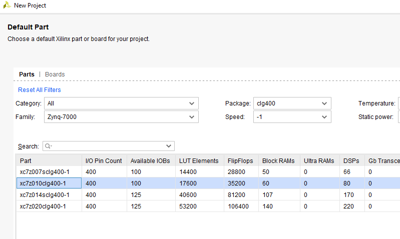
To start off, I downloaded/installed the Xilinx Vitis and Vivado tool sets. I created a new project and selected the FPGA part on my development board, the Zynq7010CLG400.
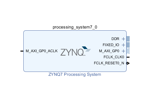
I created a block design and brought in the Zynq7000 processing system.
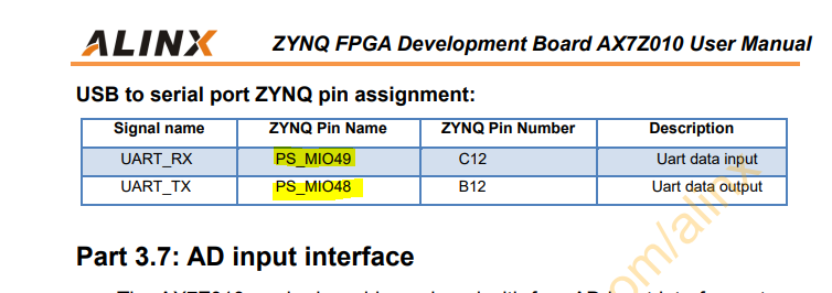
Per the development kit documentation, there is a built-in USB-UART interface on Zynq pins C12 and B12, PS_MIO49 and PS_MIO48 respectively
Double clicking on the Zynq7000 IP block brings up the configuration window. I enabled the PSUART1 peripheral at PS_MIO49 and PS_MIO48. This UART interface will be useful when debugging software later.
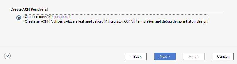
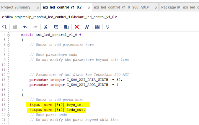
Using the tools menu, “Create and Package New IP” option, I created a new AXI4 peripheral IP block. This IP will be contain the LED control module. I configured the block to have four memory mapped registers that can be read and written over the AXI bus.
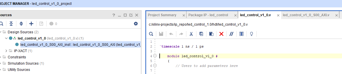
Right clicking on the peripheral block gives the option to edit the IP in a new Vivado instance. Two source files are generated. The top module just maps to the module below in the hierarchy. The child file creates a module that handles the AXI bus operations, including reads and writes from four slave registers.
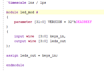
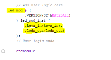
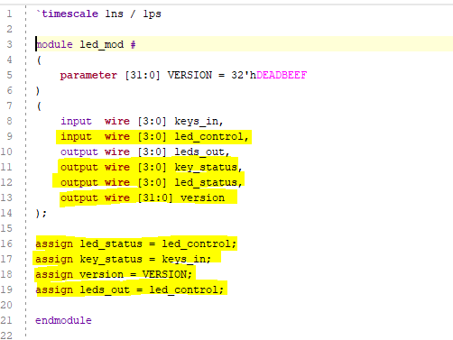
I created a new module to handle the LED control operations. Initially, all it did was wire four bits of input to four bits of output, keys_in and leds_out, respectively. Additionally, I added a version constant that will allow software to identify the firmware.
I instantiated this module in the AXI module. I mapped keys_in and leds_out to wires of the same name. Additionally, I overloaded the firmware version. This was mostly to exercise the parameter functionality in Verilog. I suppose this could be useful to allow this IP block to be shared in multiple higher level modules, each providing a unique identifier.
I added these two wires as inputs and outputs to the AXI module.
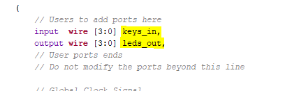
Similarly I added two wires to the top level module and connected them in the instantiation of the AXI module.
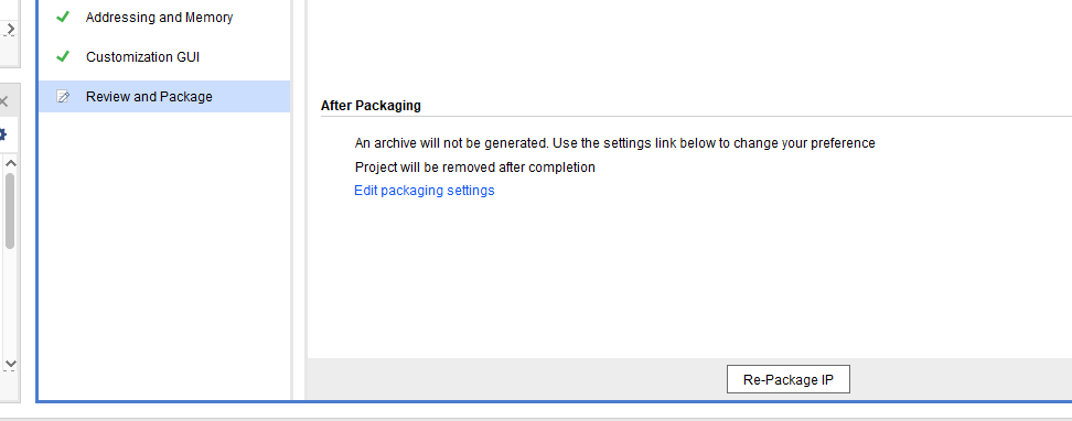
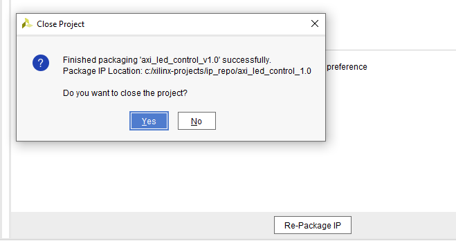
After merging in the changes in the IP packaging window, I packaged the IP and closed the project. Next I upgraded the block in the block design view of the original project.
I used the “Block Automation” feature of Vivado to handle configuring and connecting the AXI IP, the LED control IP and the Zynq processing system.
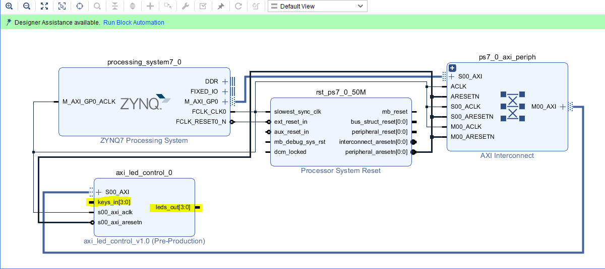
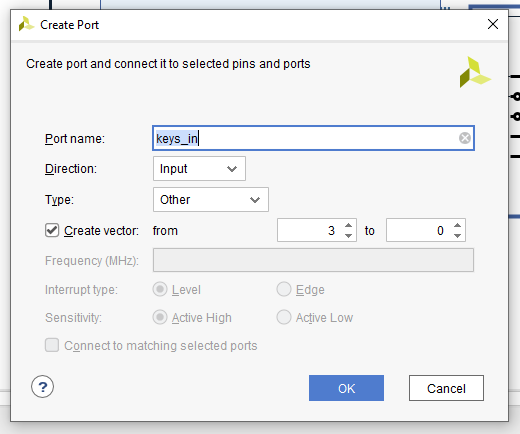
Next I created input and output ports of the same 4-bit width and wired them to the input and output of the LED control IP block.
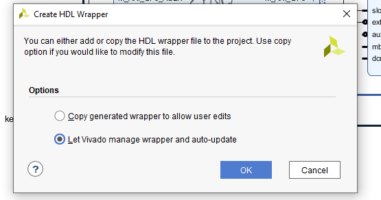
I used the “Create HDL Wrapper” option from the context menu on the block design to prompt Vivado to generate a managed HDL wrapper for the design.
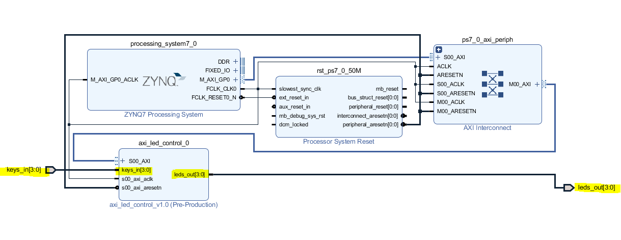
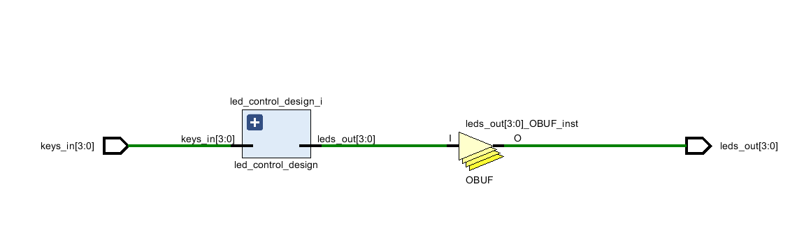
Next I synthesized the design and ran the implementation step. The schematic below shows the resulting connections.
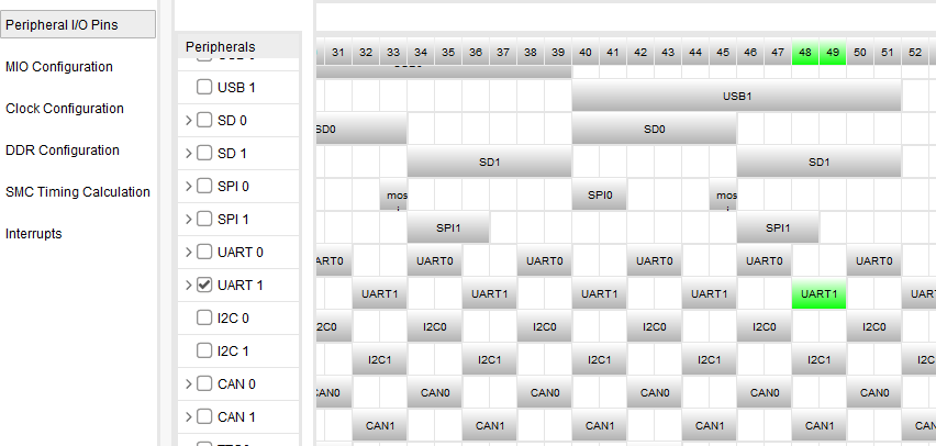
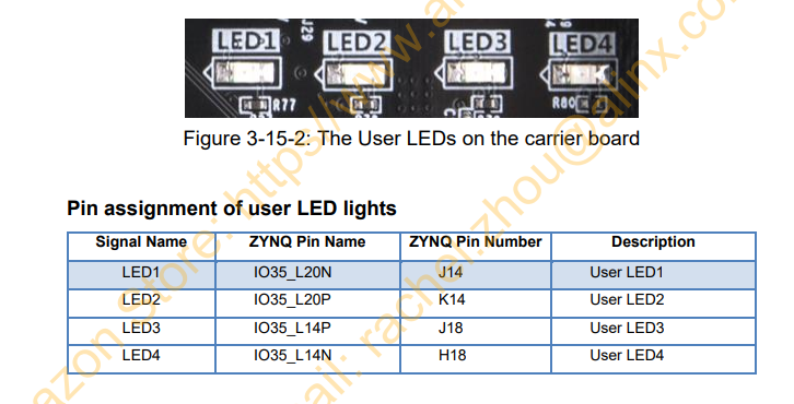
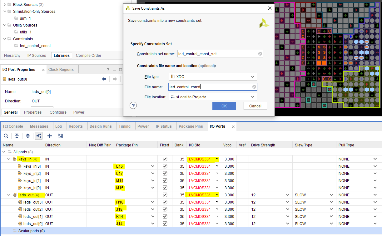
The next step was to determine the IO planning needed to connect the IP to the physical FPGA pins that correspond to the LEDs and switches. I referenced the documentation of the development kit to identify the LED pin mappings.
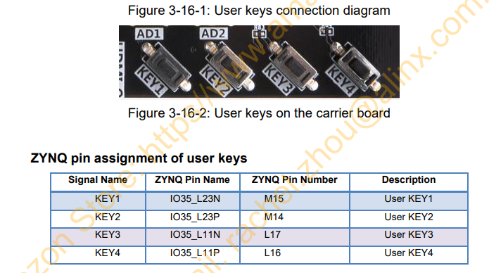
I did the same for the user key pin assignments.
I used the IO planning/IO port configuration view in Vivado to make the pin assignments. The schematic of the development kit shows that the LEDs are on a 3.3 volt rail so I set the IO standard of the switches and the LED pins to 3.3 volts.
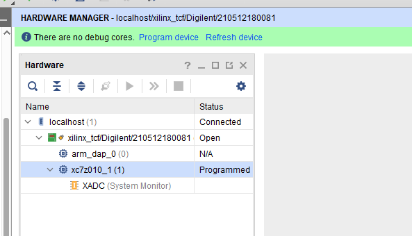
I re-ran the implementation step, generated the bitstream, and opened the hardware manager. The development kit was connected to my PC via a JTAG programming cable and powered on.
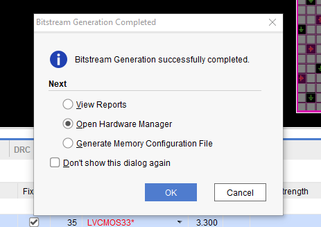
I programmed the FPGA with the bitstream.
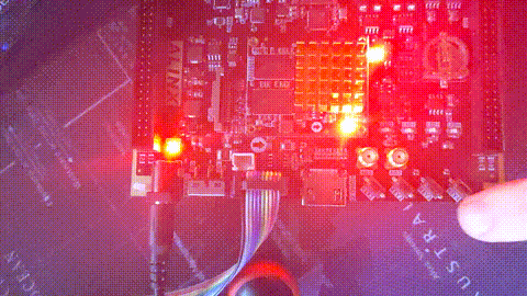
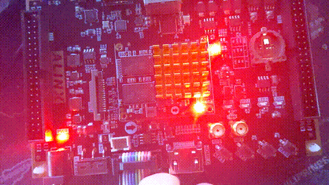
So far, all of this CDL does is match the keys to their respective lights, as seen in the GIF below.
To utilize the memory mapped AXI registers, I opened up the block design and opened the LED control IP block in the IP packager. I added several new inputs and outputs to the LED control module, in addition to the keys_in and leds_out wires.
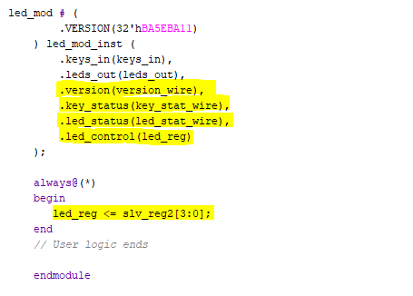
led_control – this wire is used as the four control bits for the LEDskey_status – this wire will provide the state of the four user keysled_status – this wire will provide the current state of the LEDsversion – this wire will provide the 32-bit version dataNext, led_status is connected to the led_control bit input. Similarly, key_status is connected to the keys_in bit input. The version wire is hard wired to the version parameter. Lastly, the led output bits are assigned to the led_control bit input.
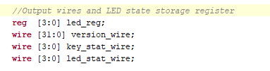
I added wires for the key status, led status, and version to the AXI module. I created a register for the LED control and status bits.
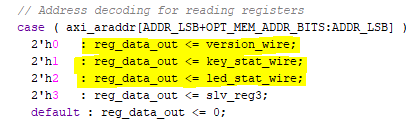
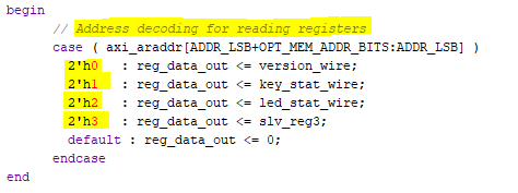
Within the auto-generated AXI code, I mapped these wires to the memory mapped registers.
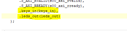
In the instantiation of the LED control module, I assigned these wires to their respective inputs and outputs. I assigned the led register to the led_control input. Lastly, I assigned the third AXI slave register to the led_reg field.
To summarize, an AXI read of the version register will return the VERSION parameter in the instantiation of the LED module. A read of the next register will return the current state of the user keys. A read of the third register will return the state of the LED register. A write to the third register will set the bits in the LED register and, in turn, control the led_out port.
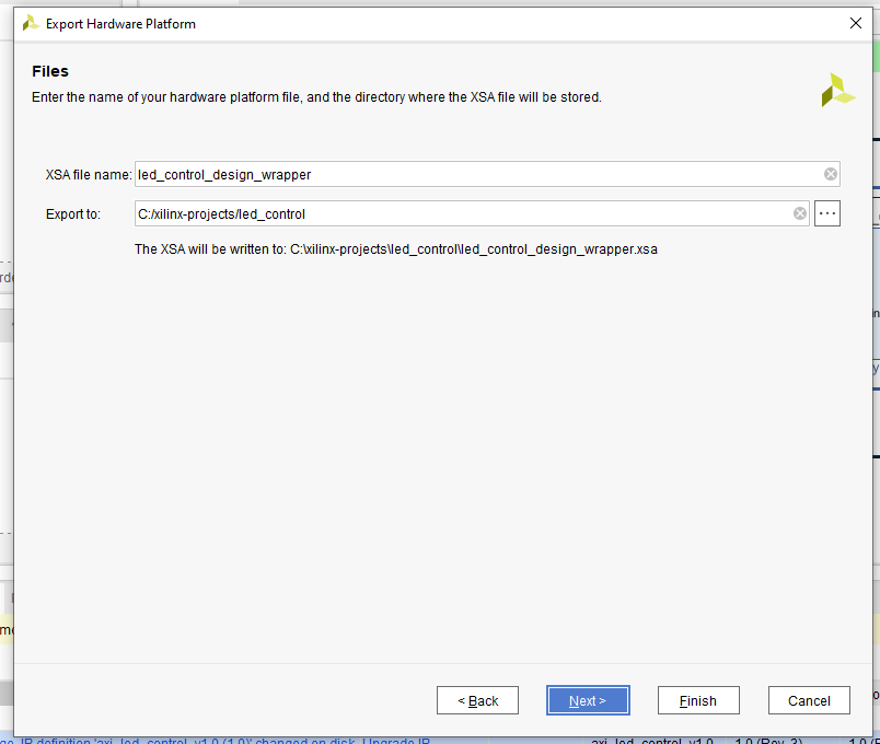
Next I repackaged the IP and closed the project. After re-synthesizing and re-implementing the design, I used the export hardware option in the file menu to export the hardware and bitstream. From the tools menu, I launched the Vitis software development IDE.
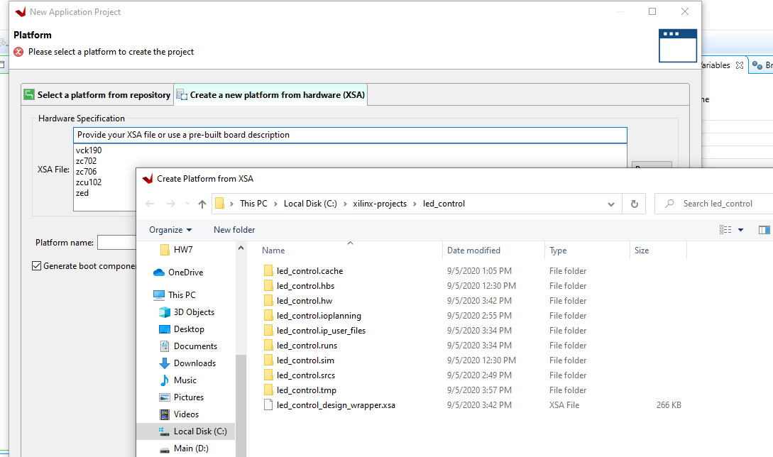
I created a new Application Project in Vitis, selecting the hardware exported in the previous step.
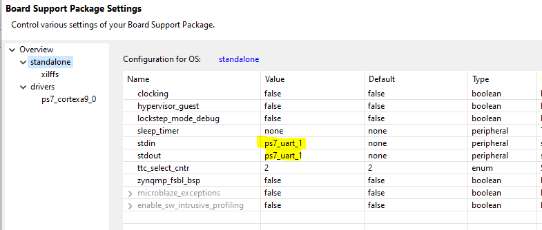
I opened up the board support package settings to ensure that stdin and stdout were mapped to the PS UART device that I previously configured in the design to map to the on-board USB-UART interface.
I opened up the hardware file to find the base address of the LED AXI peripheral.
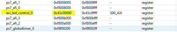
Referencing the AXI verilog, it’s clear that the four slave registers are at four consecutive addresses.
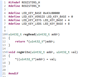
I created a registers header file with the addresses of the four slave registers, based on the peripheral base address, assigned to meaningful names. I added two convenience routines for reading and writing to/from the registers.
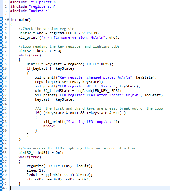
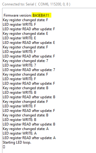
Next I created a simple C++ program to exercise the registers. First, I read the version register and print the version information. Next the application enters a loop that reads the key state register and updates the LED control register to light up the corresponding LED. If the first and third keys are pressed at the same time, the application breaks out of the first loop and enters the second loop. This loop manipulates the bits in the LED control register to scan across, lighting each LED for one second at a time.
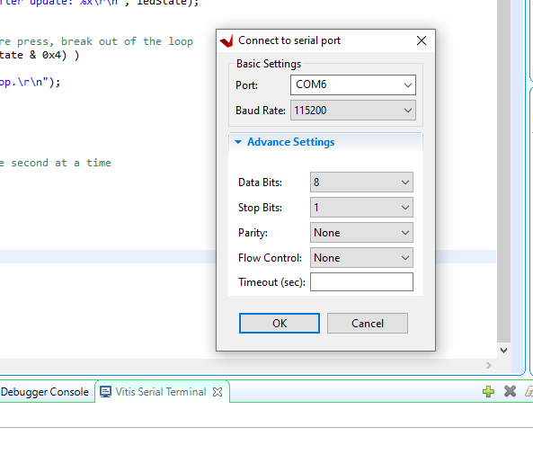
I opened up the USB-Serial interface with the Vitis serial console and ran the application with the debugger.
Below is a GIF of the application behavior.
Below is the output over the UART.
This simple project required learning some basics of CDL development and implementation; specifically the Xilinx tool set and an introduction to Verilog. I look forward to learning more and hopefully creating some projects that are actually useful and I’ll continue to write posts about them.