In this post, I cover my first attempts at working with the AXI-4 protocol to move data to and from different parts of the system; specifically, between the DDR memory and the programmable logic on my Zynq7000 development board. This topic is a necessary, missing piece of my cryptography implementations. (Not to mention that I've become aware of numerous flaws/inefficiencies in my previous cryptography blocks that I will have to revisit in future posts.) I began with Xilinx's AXI-4 Master example code and modified it to provide a memory-like interface to my IP block. I acknowledge the fact that this implementation (4 byte, single-burst-only) design underutilizes/undersupports the AXI protocol. However, this was a good starting point for me to get more experience with the AXI protocol and Xilinx's templates/verification IP.
I'm not going to cover the AXI protocol in detail because I'm far from an expert. I've utilized several web resources (references below) and Xilinx's auto-generated AXI-4 master implementation to create my memory-like interface. Briefly though, the AXI-4 protocol consists of an address channel and a data channel for both read and write operations. Two devices, slave and master, perform a handshake on these channels uing ready and valid signals. An address is provided across the address channel, and the data is transfered in bursts of words. The AXI-4 protocol supports a range of burst sizes from 1 to 256 bytes.
My design simplifies the AXI-4 transfer process into a single 32-bit word read or write. One side of the block is a full AXI-4 master interface. The other side is a block-ram-like interface. The memory interface consists of an address register (AIF_ADDR), data output register (AIF_RDATA), data input register (AIF_WDATA), write enable bit (AIF_WEN) and done/error signals (AIF_DONE, AIF_ERR). To read a word, a client sets the write enable bit low, the desired address into the address register, and enables the module. The AXI-4 master initiates a transfer from the slave and populates the read data register and asserts the AIF_DONE signal. To write a word, a client sets the write enable bit high, populates the write value, writes the target address to the address register, and enables the module. The AXI-4 master initiates the transfer to the slave and asserts the AIF_DONE signal when the write is complete.
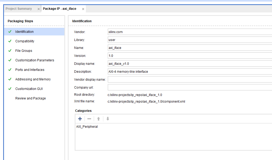
I created my design using the Xilinx "AXI-4 Full Master" peripheral template. To begin, I created a new project and used the "create and package new IP" menu option to create a new AXI-4 peripheral.
First, I modified the configurable parameter for the AXI burst length, C_M00_AXI_BURST_LEN. My design will only support single-burst transfers, so I restricted this field to a value of 1 and hid it from the Vivado GUI customization menu.
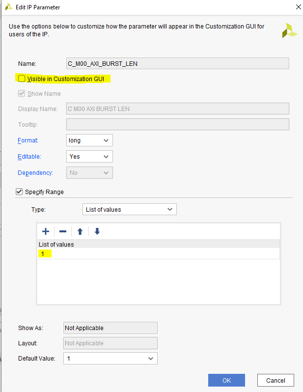
First, in the top-level wrapper, I changed the AXI burst size parameter default to single burst.
    // Parameters of Axi Master Bus Interface M00_AXI
    parameter integer C_M00_AXI_BURST_LEN   = 1,
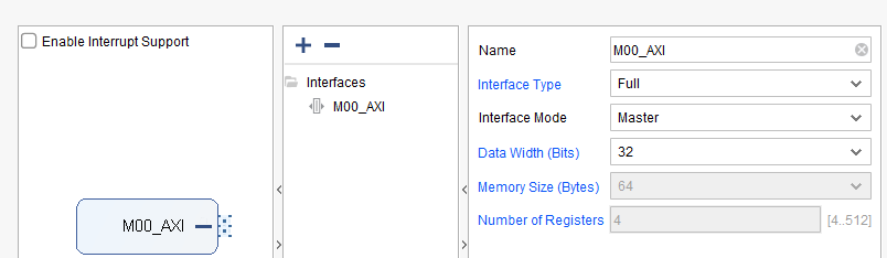
Next, I added the ports as described above.
    input [31:0] AIF_ADDR,
    //Data out (read), set to value of M_AXI_RDATA
    output wire [31:0] AIF_RDATA,
    //Data in (write)
    input [31:0] AIF_WDATA,
    //Write-enable (R or W mode)
    input AIF_WEN,
    //Indicates operation is complete, replaces TXN_DONE
    output wire AIF_DONE,
    //Indicates an error occured, replaces ERROR
    output wire [31:0] AIF_ERR,
    //Enable transactions, replaces INIT_AXI_TXN
    input AIF_EN,
I removed three signals that the Xilinx template includes that aren't needed, m00_axi_init_axi_txn, m00_axi_txn_done and m00_axi_error. I then added these ports to the instance of the AXI module.
axi_iface_v1_0_M00_AXI_inst (
        .AIF_ADDR(AIF_ADDR),
        .AIF_RDATA(AIF_RDATA),
        .AIF_WDATA(AIF_WDATA),
        .AIF_WEN(AIF_WEN),
        .AIF_DONE(AIF_DONE),
        .AIF_ERR(AIF_ERR),
        .AIF_EN(AIF_EN),
In the underlying module, I made the same change to the burst length parameter, added the new ports, and removed the same unused signals. I changed the C_NO_BURSTS_REQ local parameter to reflect the single-only burst length.
    // Number of bursts is always 1
     localparam integer C_NO_BURSTS_REQ = 1;
The default template state machine, when enabled, performs a sequential write operation, reads the values back, and compares the read values to the expected values. I modified the state machine to perform a read or write (depending on the write enable signal) and then wait for the operation to complete before indicating either "done" or "error". I created a new state for this, CHECK_DONE.
    parameter [1:0] IDLE = 2'b00, // This state initiates the transaction
        // after the state machine changes state to INIT_WRITE
        // when there is 0 to 1 transition on INIT_AXI_TXN
        INIT_WRITE   = 2'b01, // This state initializes write transaction,
        // once writes are done, the state machine
        // changes state to CHECK_DONE
        INIT_READ = 2'b10, // This state initializes read transaction
        // once reads are done, the state machine
        // changes state to CHECK_DONE
        CHECK_DONE = 2'b11; // This state issues the status of the operation, replaces INIT_COMPARE
I replaced the single-bit error register with a 32-bit register, error_reg, to support error codes. I removed two registers, compare_done and read_mismatch from the template code. I modified the template's write address wire, M_AXI_AWADDR, and read address wire, M_AXI_ARADDR, to use the AIF_ADDR input signal.
    //The AXI address is a concatenation of the target base address + active offset range
    assign M_AXI_AWADDR = C_M_TARGET_SLAVE_BASE_ADDR + AIF_ADDR;
    ...
    assign M_AXI_ARADDR = C_M_TARGET_SLAVE_BASE_ADDR + AIF_ADDR;
I assigned the AIF_DONE signal to either the writes_done or reads_done register, depending on the mode.
assign AIF_DONE = (AIF_WEN == 1) ? writes_done : reads_done;
The template includes an always block to initiate the AXI transaction. I modified it to utilize my AIF_EN signal.
    //Generate a pulse to initiate AXI transaction.
    always @(posedge M_AXI_ACLK)
      begin
        // Initiates AXI transaction delay
        if (M_AXI_ARESETN == 0 )
          begin
            init_txn_ff <= 1'b0;
            init_txn_ff2 <= 1'b0;
          end
        else
          begin
            init_txn_ff <= AIF_EN;
            init_txn_ff2 <= init_txn_ff;
          end
      end
I removed unused always blocks that were used to generate sequential write and read addresseses that the example logic required. I also removed an always block that was used to compare the read-back data to the expected values. Another always block was used to assign and increment the AXI write data for the example logic. I modified this block to assign the externally provided write data, AIF_WDATA.
    /* Set the write data to the input write data */
    always @(posedge M_AXI_ACLK)
    begin
        axi_wdata = AIF_WDATA;
    end
I modified an error-checking always block to populate my error register in the event of a failed read or write, based on the AXI read/write response signals.
      always @(posedge M_AXI_ACLK)
      begin
        if (M_AXI_ARESETN == 0 || init_txn_pulse == 1'b1)
          begin
            error_reg <= 1'b0;
          end
        else if (write_resp_error || read_resp_error)
          begin
                if(write_resp_error)
                    error_reg <= 8'b1;
                else
                    error_reg <= 8'b10;
          end
        else
          error_reg <= error_reg;
      end
Next, I modified the example state machine to perform read/write operations as described above. I added logic to clear the AIF_ERR register on reset to the reset section of the block. I modified the IDLE state to transition to either the INIT_READ or INIT_WRITE state, depending on the selected mode.
      always @ ( posedge M_AXI_ACLK)
      begin
        if (M_AXI_ARESETN == 1'b0 )
          begin
            // reset condition
            // All the signals are assigned default values under reset condition
            mst_exec_state      <= IDLE;
            start_single_burst_write <= 1'b0;
            start_single_burst_read  <= 1'b0;
            AIF_ERR <= 1'b0;
          end
        else
          begin

            // state transition
            case (mst_exec_state)

             IDLE:
                // This state is responsible to wait for user defined C_M_START_COUNT
                // number of clock cycles.
                if ( init_txn_pulse == 1'b1)
                  begin
                    if(AIF_WEN)
                        mst_exec_state  <= INIT_WRITE;
                    else
                        mst_exec_state <= INIT_READ;
                    AIF_ERR <= 1'b0;
                  end
                else
                  begin
                    mst_exec_state  <= IDLE;
                  end
The INIT_WRITE and INIT_READ states remained largely unchanged other than modifying the transition to enter my new CHECK_DONE state. In the CHECK_DONE state, the error output register, AIF_ERR is set to the value of the error_reg register and the state mahcine transitions back to IDLE. The actual read/write logic is still performed by the Xilinx boilerplate code, as is the error checking. Lastly, I added an always block to assign the AXI read data, M_AXI_RDATA to the output register, AIF_RDATA, when the read data is valid as indicated by the rvalid and rready signals.
    //This block is responsible for latching the read data into the RDATA register
    always @(posedge M_AXI_ACLK)
    begin
        if(M_AXI_RVALID && axi_rready) begin
            AIF_RDATA <= M_AXI_RDATA;
        end
    end
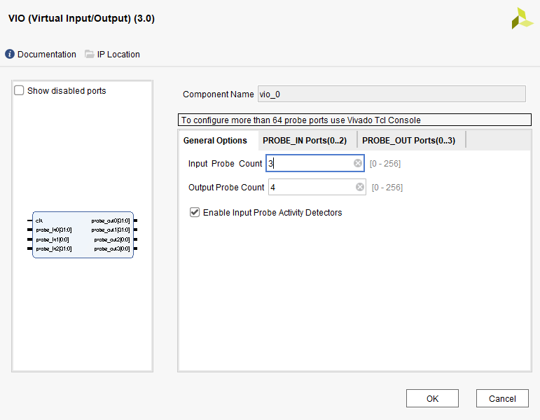
To test this module, I began by creating a block design for the Zynq7000. I utilized Xilinx's Virtual Input Output (VIO) IP core. This IP allows for reading and writing to signals via JTAG in the Vivado hardware manager. I created a VIO block and added probes for each of the AIF_* signals on the AXI interface.
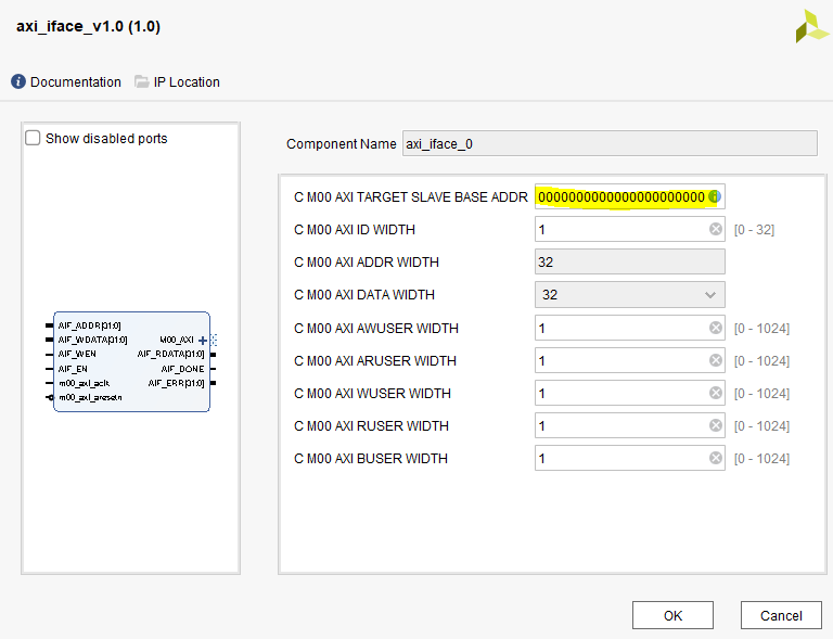
I set the target slave base address to 0. The AXI interface module's AIF_ADDR field is an offset from the target slave base address. Setting it to 0 allowed me to write absolute addresses, but I could have also set this to the base address of the actual target, in this case, the external DDR.
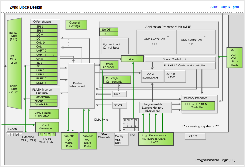
As seen in the block diagram below, the Zynq7000 has four AXI high performance slave ports that provide a path to the DDR memory controller. I enabled the HP0 port and connected it to the AXI interface master port.
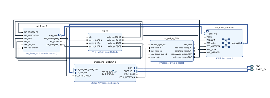
The image below is the final block design for the system. The VIO probes are connected to each of the ports on the AXI interface block.
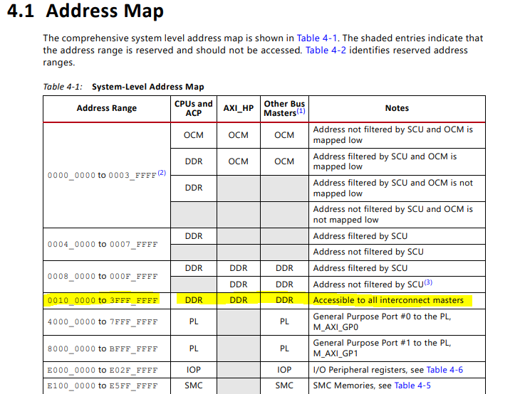
I created a minimal sofware application to bring the Zynq processing system up and interact with the DDR memory. The Technical Reference Manual (TRM) for the Zynq contains an address map indicating that the AXI HP slave ports, as well as the processing system, can access the DDR from address 0x001000000.
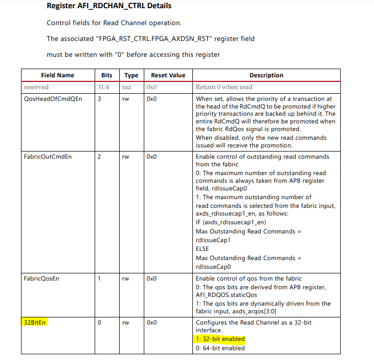
Additionally, to enable 32-bit mode on the HP port, the TRM shows that the AFI_RDCHAIN_CTRL register, bit 0, must be set.
The software application was created in the Vitis IDE using the hello world C template. It starts by creating a pointer to the DDR address range mentioned above and setting the requisite bit in the AFI_RDCHAIN_CTRL register.
    //Address is RAM from PS and PL perspective
    uint32_t * dataPtr = (uint32_t*)0x00100000;

    //Set HP0 to 32-bit mode
    uint32_t * afiRdChain = (uint32_t*)0xF8008000;
    *afiRdChain = (*afiRdChain) | 1;
First, the application writes some arbitrary sequential values to the DDR. After the writes, the cache memory is flushed. If this step isn't performed, the processor memory reads will come from cache, unaware of values written to the DDR by the PL and vice-versa. Xilinx provides an AXI port that supports cache coherency in a much more efficient manner, something I plan to look into more in the future.
//Write some values
*dataPtr = 0xAA;
for(int i = 0; i < 10; i++)
{
*(dataPtr + i) = 0xAA + i;
}
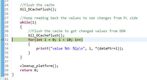
//Flush the cache
Xil_DCacheFlush();
Next, I enter an infinite loop that reads and prints the same memory locations, clearing the cache on each iteration. I ran the application on the hardware in debug mode, setting a break point on each iteration of this loop. The section below shows the serial terminal output after the first iteration of the loop.
    //Keep reading back the values to see changes from PL side
    while(1)
    {
        //Flush the cache to get changed values from DDR
        Xil_DCacheFlush();
        for(int i = 0; i < 10; i++)
        {
            printf("value %d: %lx\n", i, *(dataPtr+i));
        }
    }
value 0: aa
value 1: ab
value 2: ac
value 3: ad
value 4: ae
value 5: af
value 6: b0
value 7: b1
value 8: b2
value 9: b3
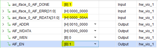
With the board running, the Vivado hardware manager view shows the VIO probes that were added to the design.

The VIO interface allowed me to manually manipulate the AXI interface. First, I pointed it to the DDR memory address via the AIF_ADDR field.
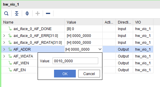
I enabled the interface by setting the AIF_EN bit and the value at the input address was read and populated into the AIF_RDATA register. The AIF_DONE signal indicated that the operation was completed and the AIF_ERR register did not indicate an error.
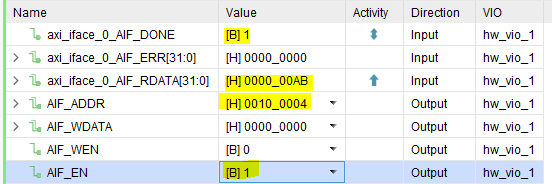
Next, I incremented the AIF_ADDR field to the next address and toggled the AIF_EN bit to initiate another read.
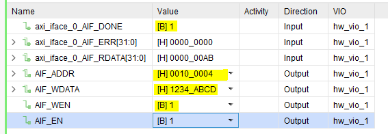
Next, I populated the AIF_WDATA field, set the write enable bit, AIF_WEN and toggled the enable signal to initiate a write. As before, the module indicated "done" with no error.
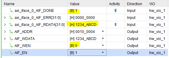
Next, I read back the same address location by clearing the write-enable bit and re-enabling the module. The expected value was read back.
I returned to the Vitis IDE and let the print loop complete another iteration. The output reflects the value just written from the PL.
value 0: aa
value 1: 1234abcd
value 2: ac
value 3: ad
value 4: ae
value 5: af
value 6: b0
value 7: b1
value 8: b2
value 9: b3
This interface, and the research it required for me to implement it, has given me an introductory understanding of the AXI-4 protocol. I intend to use this interface in a proof-of-concept design synthesized and run on the Zynq7000 development board that I will cover in a future post. I intend to refine this design and tailor it to for use as the primary data path for my cryptography implementations (at least until a streaming solution is required).