This is a continuation of my previous post. I built a simple proof-of-concept system that uses the AXI interface I covered in my previous post to read, alter, and write back data stored in the Zynq7000 DDR. The software application running in the Zynq7000 processing system (PS) writes data to the DDR, informs the programmable logic (PL) module of the data location and number of 32-bit words, and then enables the module. The module reads the given number of words from the specified address, calculates the logical negation (flips the bits), and writes the words back to the DDR. The PS control of the module is done over memory mapped AXI registers, controlled by the PS AXI master. The data transfer to DDR is done by the PL AXI master over the PS high performance AXI slave.
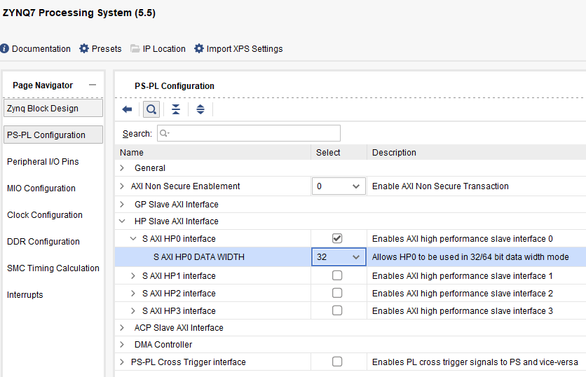
To begin, I created a block design for the system and added the Zynq7000 processing system, enabling the high performance AXI slave port as I did in my previous post.

Next, I added a new AXI slave peripheral for the bit flipper using Vivado's AXI slave template. In addition, the AXI interface, I added the signals required to interact with the AXI memory-like interface I created in my previous post. The requisite ports were added to the top-level module and connected in the instantiation of the underlying IP block.
// Users to add ports here
        output wire [31:0] AIF_ADDR,
        output wire [31:0] AIF_WDATA,
        output wire [0:0] AIF_WEN,
        output wire [0:0] AIF_EN,
        input wire [0:0] AIF_DONE,
        input wire [31:0] AIF_ERR,
        input wire [31:0] AIF_RDATA,
...
        .AIF_ADDR(AIF_ADDR),
        .AIF_WDATA(AIF_WDATA),
        .AIF_WEN(AIF_WEN),
        .AIF_EN(AIF_EN),
        .AIF_DONE(AIF_DONE),
        .AIF_ERR(AIF_ERR),
        .AIF_RDATA(AIF_RDATA)
In the underlying module, I added the same ports.
    // Users to add ports here
    output reg [31:0] AIF_ADDR,
    output reg [31:0] AIF_WDATA,
    output reg [0:0] AIF_WEN,
    output reg [0:0] AIF_EN,
    input  [0:0] AIF_DONE,
    input  [31:0] AIF_ERR,
    input  [31:0] AIF_RDATA,
Toward the bottom of the file, before the read selection logic, I added registers for control and state information.
    //Bitflipper
    reg [7:0] state_reg;  //State information for bit flipper state machine
    reg [31:0] debug_reg; //Debug value register
    reg error;            //Error register
    reg done;             //Done signal register
    reg init_ff;           //Init pulse
    reg init_ff2;
    wire init_pulse;       //Init wire
    reg [31:0] word_counter;  //Counter for 32-bit words
    reg [31:0] num_words;     //Number of words to flip
    reg [31:0] current_addr;  //Current address
state_reg - holds the current state of the main state machinedebug_reg - Used to pass debug information to the PS sideerror - Set if an error occursdone - Set when the operation is completeinit_ff, init_ff2 - Borrowed from Xilinx template code, used as a single-clock pulse to start the state machineinit_pulse - Wire that triggers the state machineword_counter - Tracks how many 32-bit words have been flippednum_words - Latched with the number of 32-bit words requestedcurrent_addr - Stores the address of the current wordNext, I added flags for the state machine states.
    //State machine flags
    localparam [3:0] IDLE = 4'h0,
                     READ = 4'h1,
                     WAIT_READ = 4'h2,
                     WRITE = 4'h3,
                     WAIT_WRITE = 4'h4,
                     FINAL = 4'h5;
IDLE - The initial stateREAD - Perform a read of the word at current_addrWAIT_READ - Wait for the read to complete or errorWRITE - Write the negated word back to current_addrFINAL - The final stateNext, I added an initial block to initialize all the registers. I modified the Xilinx template code read logic to pass information to the PS side. A read at the first register returns a "version" value, in this case, the date. This is mostly just a sanity check to make sure the module is working. The next register is the "control" register; on read, bit 0 is the "done" flag, and bit 1 is the "error" flag. A read at the third register returns the value of the debug register.
    // Address decoding for reading registers
    case ( axi_araddr[ADDR_LSB+OPT_MEM_ADDR_BITS:ADDR_LSB] )
    2'h0   : reg_data_out <= 32'h12302020; //Version Register, RO
    2'h1   : reg_data_out <= {30'b0, error, done};
    2'h2   : reg_data_out <= debug_reg;
In the user logic section, I added an always block to kick off the state machine whenever the enable bit transitions to 1 in the control register (slv_reg1). Structuring the initialization this way ensures that the state machine will run exactly one time per-enable. The init wire is used to route this initialization pulse.
    // Add user logic here
    assign init = (!init_ff2) && init_ff;

    //Initialization pulse for the bit flip state machine
    always @(posedge S_AXI_ACLK)
      begin
        // Start the bit flip state machine
        if (S_AXI_ARESETN == 0)
          begin
            init_ff <= 1'b0;
            init_ff2 <= 1'b0;
          end
        else
          begin
            init_ff <= slv_reg1[0];
            init_ff2 <= init_ff;
          end
      end
Next, I added an always block for the state machine. First, I added a reset section at the top to reset the registers. The state machine demonstrates how I intend to use the AXI memory-like interface. The initial state waits for the init signal and latches the PS-provided address and word count into the current_addr and num_words register. Additionally, it clears the done and error registers and resets the word counter.
case(state_reg)
            //Idle state waits for init and sets up the first read
            IDLE: begin
                if(init == 1) begin
                    done <= 0;
                    error <= 0;
                    word_counter <= 0;
                    current_addr <= slv_reg2;
                    num_words <= slv_reg3;
                    state_reg <= READ;
                end
            end
The read state clears the write-enable bit of the AXI interface, sets the address and enables it to initiate a read before transitioning to the WAIT_READ state.
            //Read state performs the read
            READ: begin
                AIF_WEN <= 0;
                AIF_ADDR <= current_addr;
                AIF_EN <= 1;
                state_reg <= WAIT_READ;
            end
The WAIT_READ state loops until either the done or error signals are set on the AXI interface. In the case of an error, the "error code" returned form the interface is stored in the debug register and the state machine transitions back to IDLE. If the operation succeeds, the state machine transitions to the WRITE state.
            //Wait for done or error
            WAIT_READ: begin
                if(AIF_DONE == 1) begin
                    AIF_EN <= 0;
                    state_reg <= WRITE;
                end
                else if(AIF_ERR != 0) begin
                    error <= 1;
                    state_reg <= IDLE;
                    debug_reg <= AIF_ERR;
                end
                else
                    state_reg <= WAIT_READ;
            end
In the write state, the AXI interface is set up to perform a write by setting the write-enable bit and enabling the module. The state machine then transitions to the WAIT_WRITE state.
            //Write back flipped bits
            WRITE: begin
                AIF_WDATA <= ~AIF_RDATA;
                AIF_WEN <= 1;
                AIF_EN <= 1;
                state_reg <= WAIT_WRITE;
            end
The WAIT_WRITE checks for "done" or "error" the same way as WAIT_READ before incrementing the word counter and transitioning to the FINAL state.
            //Wait for done or error
            WAIT_WRITE: begin
                if(AIF_DONE == 1) begin
                    AIF_EN <= 0;
                    state_reg <= FINAL;
                    word_counter <= word_counter + 1;
                end
                else if(AIF_ERR != 0) begin
                    error <= 1;
                    state_reg <= IDLE;
                    debug_reg <= AIF_ERR;
                end
                else
                    state_reg <= WAIT_WRITE;
            end
The FINAL state checks the word count against the total number of words. If there are words left to flip, the state machine increments the address and returns to the READ state; otherwise, the done register is set and the state machine returns to the IDLE state.
            //Loop if there are more words to flip, or return to idle
            FINAL: begin
                if(word_counter < num_words) begin
                    current_addr <= current_addr + 32'h4;
                    state_reg <= READ;
                end
                else begin
                    done <= 1;
                    state_reg <= IDLE;
                end
            end
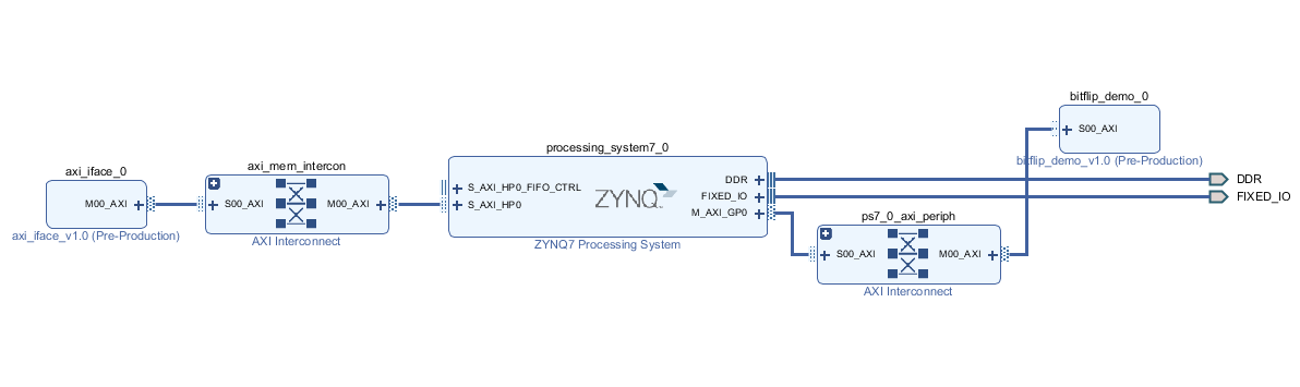
I packaged the module and returned to the main block design for the Zynq. As in my previous post, I brought in the AXI interface and configured the base slave address to 0. Subsequent addresses passed to the modules are offsets from this address (and as a result of the base address of 0, essentially absoulte addresses).

Adding the bit flipper module and running the Vivado connection automation results in the final block design (only interfaces shown in the image below). I synthesized and exported this platform.
I created an empty C++ software application project in the Vitis IDE to drive the bit flipping module based on the hardware specification described above.

I spent a little extra time on the software application so I can use it as a template for similar projects going forward; there are, however, a few design decisions I skipped over for convenience, which I'll mention below.
I began by defining a base class to encapsulate register operations. I created a register template that takes the register address as a parameter. I created read/write, read-only, and write-only classes that only support those operations. This is useful because I've chosen to allow some registers to behave differently depending on which operation is performed. For example, the offset register is write-only. A read at the same address returns the debug information, and, as a result, the debug register is read-only. I'd like to refine this register class to enforce a singleton construction pattern and mutual exclusion to prevent multiple instances of the class reading/writing to the same register.
class RegisterBase
{
protected:
    RegisterBase(uint32_t _address) : address(_address)
    {}
    uint32_t address;
public:
    ~RegisterBase(){}
};

template <uint32_t ADDR>
class RO_Register : public RegisterBase
{
public:
    RO_Register() : RegisterBase(ADDR)
    {
    }

    uint32_t read()
    {
        return *((uint32_t*)address);
    }
};

template <uint32_t ADDR>
class WO_Register : public RegisterBase
{
public:
    WO_Register() : RegisterBase(ADDR)
    {
    }

    void write(uint32_t v)
    {
        *((uint32_t*)address) = v;
    }
};

template <uint32_t ADDR>
class RW_Register : public RO_Register<ADDR>, public WO_Register<ADDR>
{
public:
    RW_Register()
    {
    }
};
Next, I added a bit flipper module-specfic set of registers to support operations on the bit flipper module. These registers are instantiated with the addresses defined in the memory map of the AXI peripheral.
RO_Register<0x43C00000> bf_version;
RW_Register<0x43C00004> bf_control;
WO_Register<0x43C00008> bf_offset;
RO_Register<0x43C00008> bf_debug;
WO_Register<0x43C0000C> bf_num_word;
I then created a class to encapsulate the bit flip module itself. This is another class that I would create as a singleton in a real application. The class has an initialization method that sets up the AXI high performance slave port on the Zynq PS (covered in my previous post). The class contains a single method to flip the bits of an array of words.
    void init();
    void flip(uint32_t * data, uint32_t len);
The constructor of the class calls the intialize method. Inside the flip function, some information is printed, including the module version, the passed data is copied into the DDR at the PL-accessible DDR address (DDR_BASE), and the cache is flushed (covered in my previous post.)
    //Print some info
    printf("Version: %lx\n", bf_version.read());
    printf("Status: %lx\n", bf_control.read());
    printf("Flipping %ld words.\n", len);

    //Copy the input data to the DDR
    for(uint32_t i = 0; i < len; i++)
    {
        *((uint32_t*)DDR_BASE + i) = data[i];
    }

    //Flush cache to DDR
    Xil_DCacheFlush();
Next the offset and number of words are written to the bitflip module via the register objects, and the module is enabled. The function then loops waiting for "done" or "error" and then flushes the cache again. This routine doesn't do any actual error checking, but the status register is printed.
    //Offset (from 0)
    bf_offset.write(DDR_BASE);

    //Number of words
    bf_num_word.write(len);

    //Enable
    bf_control.write(1);

    //Wait for done or error
    while(bf_control.read() == 0){}

    //Flush cache again to get actual DDR contents
    Xil_DCacheFlush();

    //Print status
    printf("Status after flip: %lx\n", bf_control.read());
Lastly, the data is copied back to the user-provided array. The main function of the application creates and prints an arbitrary array of words. Next it calls the flip() routine on an instance of the bit flip class. Lastly, it prints the resulting flipped values.
printf("Bit Flipper Test\n");
    BitFlipper bf;
    uint32_t flip_data[DATA_LEN] = {0x11, 0x22, 0x33, 0x44, 0x55, 0xAA, 0xBB, 0xCC, 0xDD, 0xEE};

    //Print the input data
    printf("Original: \n");
    for(uint32_t i = 0; i < DATA_LEN; i++)
    {
        printf(" %lx ", flip_data[i]);
    }
    printf("\n");

    //Flip it
    bf.flip(flip_data, DATA_LEN);

    //Print the output data
    printf("Flipped: \n");
    for(uint32_t i = 0; i < DATA_LEN; i++)
    {
        printf(" %lx ", flip_data[i]);
    }
    printf("\n");

    printf("Unflipped (software): \n");
    for(uint32_t i = 0; i < DATA_LEN; i++)
    {
        printf(" %lx ", ~flip_data[i]);
    }
    printf("\n");
Running the application on the Zynq7000 produces the following output over the serial terminal.
Bit Flipper Test
Original:
11  22  33  44  55  aa  bb  cc  dd  ee
Version: 12302020
Status: 0
Flipping 10 words.
Status after flip: 1
Flipped:
ffffffee  ffffffdd  ffffffcc  ffffffbb  ffffffaa  ffffff55  ffffff44  ffffff33  ffffff22  ffffff11
Unflipped (software):
11  22  33  44  55  aa  bb  cc  dd  ee
Obviously, this module has no real purpose, and the AXI interface is extremely inefficient, but I learned a lot in this process, and I think this will provide a good foundation to build off for future projects. I did a fair amount of debugging in the Vivado environment with the VIO and ILA IP cores which I'm certain I will use going forward. In future posts I'm going to keep improving this system and return to implementing and integrating cryptographic modules.